Semiconductor Micro-Inspection
Developing Machine Vision to inspect semiconductor defects in production.
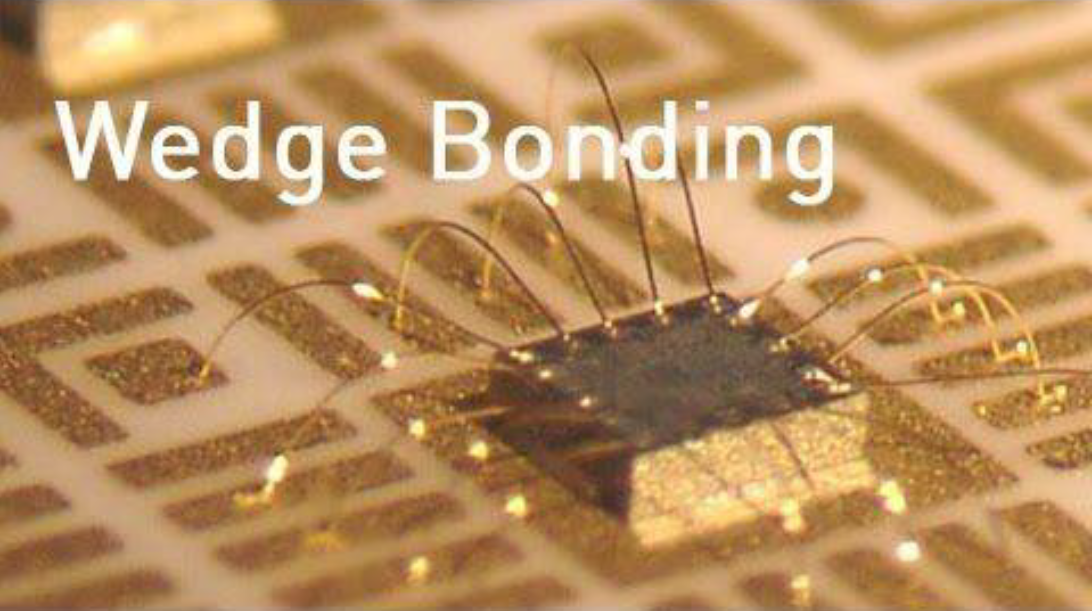
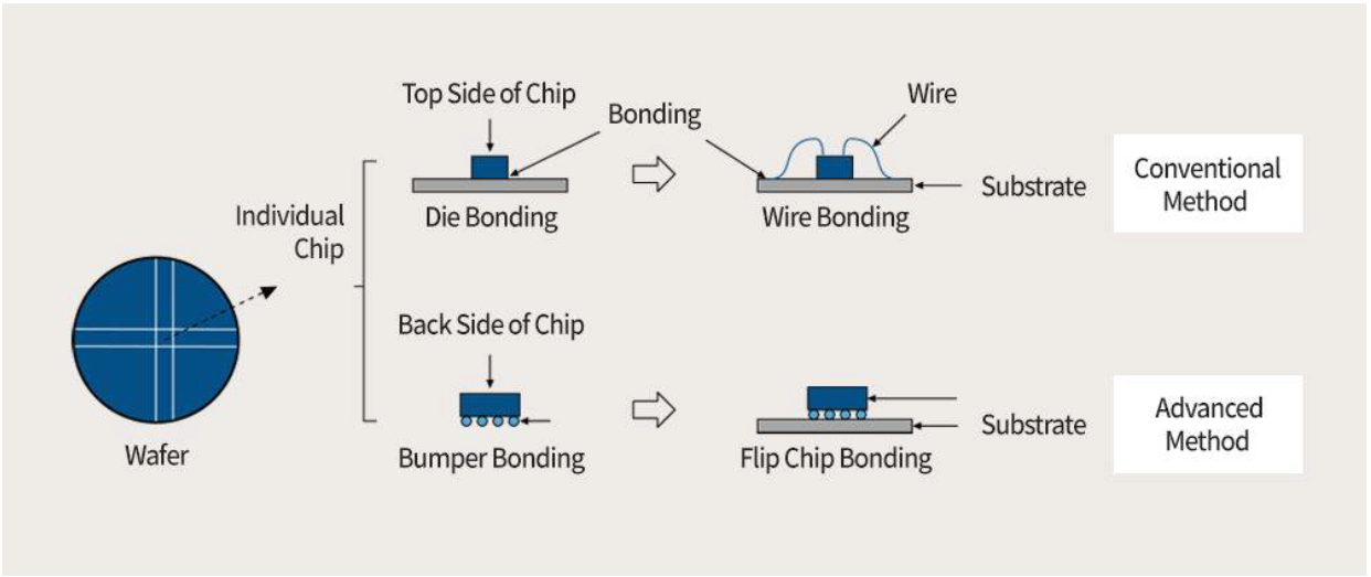
Chip bonding refers to a technique by which the individual chips of a wafer are attached to a substrate using an appropriate adhesive.
When necessary, it must maintain constant electrical conduction or realize a high level of insulation. Therefore, bonding methods are becoming more important as chips continue to become smaller and smaller.
There are many defects on:
- Substrate: contamination, displacement
- Chip: displacement, chip skew in 3D direction
- Pad (electrode) on chip and substrate: shape, location, displacement
- Epoxy: not fully covered the bonding area
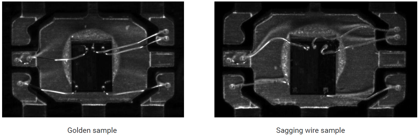
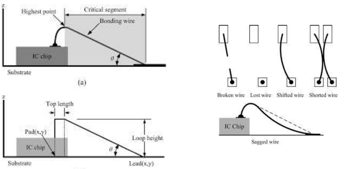
- Wire: looping, breaking, loop height, touching
Illustrated image: 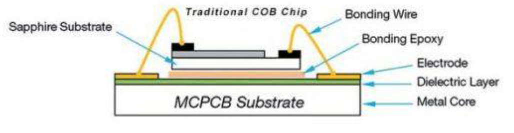
System advantages:
- On-the-fly inspection
- Contactless measurement
- Detection Yield: 99.5%
- Measurement:
- Accuracy: 8 μm
- Repeatability: 4 μm
Illumination system 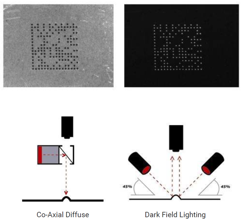
Actual samples: 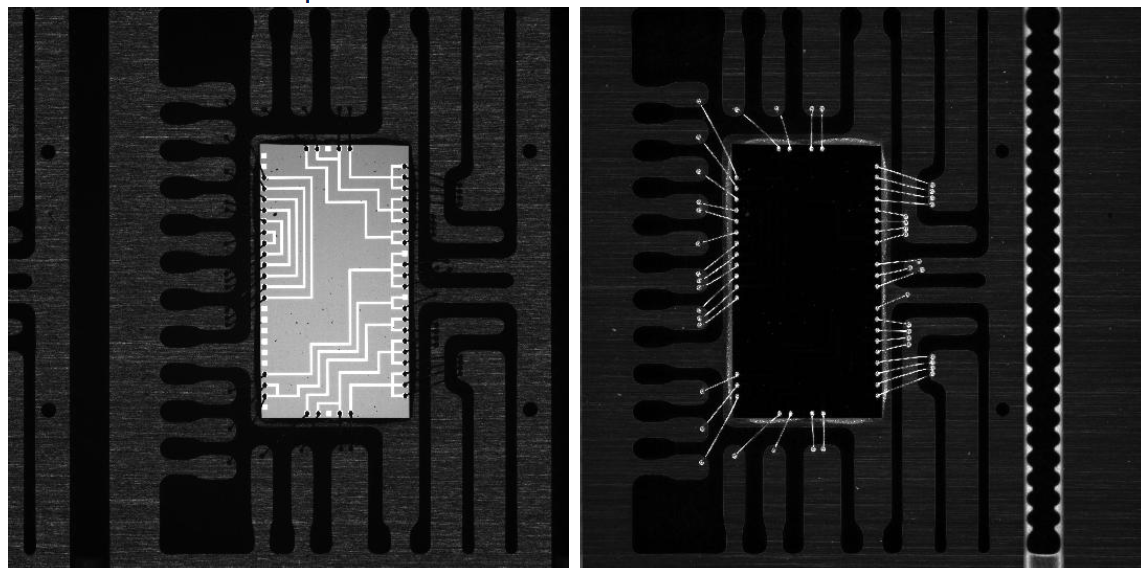
Sagging wire samples: